by Ovidiu Plugariu | Dec 17, 2021 | ASIC / FPGA Generics
I bet you’ve heard a lot about FPGAs but I feel that you’ve asked yourself: “Where are these FPGAs?“, “Have I seen one until now?“, “Are you sure that there are common applications for this types of exotic chips?“. Fact is that FPGAs are present starting from the deep bottom of the ocean (submarines) and going way far into deep space at the edge of our solar system (satellites). Let’s check out how FPGAs are used by various industries and how we silently intersect with them day-by-day.
DATA CENTERS
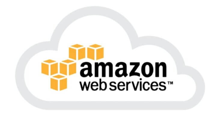
Chances are high that between you and reading this post a lot of FPGAs are involved in search engines, data compression, or data encryption. FPGAs are used in data centers because of their parallelism, high throughput and low-latency. Amazon WEB Services even lets yow rent FPGA fabric inside their datacenters and connect it with your application as a hardware accelerator (Amazon EC2 F1). Video processing, machine learning and data compression are just a few of possible applications that these FPGAs are used in the Amazon datacenters by their clients.
Sometimes FPGAs are used by large service providers like Google, Facebook or even banks to provide high quality data center services for a large amount of concurrent users. When 10k users search for different content in the same time, you need to have an extremely fast infrastructure that can accommodate them.
AUTOMOTIVE
 The modern day car accommodates a large variety of chips, like microcontrollers, CPUs, GPUs and even FPGAs. A first example for FPGA usage inside a car would be the Advanced Driver Assistance System (ADAS) which is used to give extra safety when the car is in the traffic by processing large amounts of data from various sensors (video, Lidar, pressure, temperature, motor, speed, driver gestures, etc…) and integrating them into complex algorithms to decide if the car, the driver and other traffic participants are circulating in a safe manner for everyone. An FPGA is best suited here because it can aggregate large amounts of different data types, has hundreds of I/O pins and can be reconfigured if something needs to be updated later in the production chain, or after the car is sold.
FPGAs are also used for motor control algorithms in electric / hybrid cars, in the security gateway or in the infotainment system. Since cars use so many chips the market has been highly affected by the current semiconductor crisis.
DEFENSE
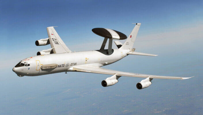 Modern military technologies use state-of-the-art electronics devices, with high requirements for quality, safety and operating conditions. FPGAs are used for radar, sonar, electronic warfare, secure communication systems, encryption, avionics control equipment, unmanned aerial vehicles, smart munitions, etc…
The key features of an FPGA that recommends it for the defense sector are: configurability, fast IO, low latency and parallel processing power of multiple sensor sources [1].
Space
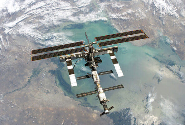 Space equipment as satellites have a lifetime of 10+ years so the chips inside them have to keep the pace with the updates of the telecom standards and algorithm updates [2]. A radiation-hardened FPGA, both by capsule materials and by the use of design techniques as Triple Module Redundancy and Hamming Codes, is a low-power reprogrammable device that can be updated with a new functionality even when the device is thousands of miles away in the harsh space environment.
The most popular applications for Space FPGA applications are: digital signal processing, high resolution optical and radar imagery, machine learning and AI [3].
Aerospace
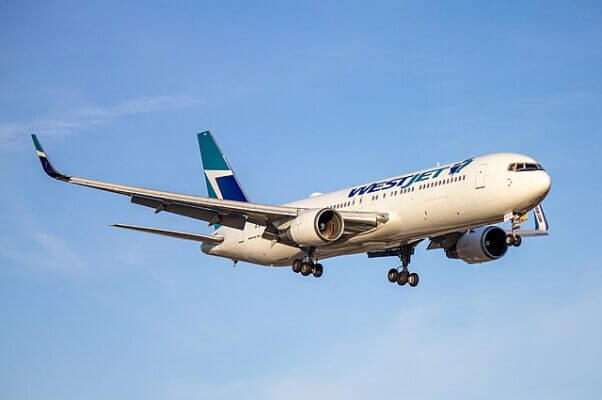 This electronics used in this field are categorized as being safety-critical because the malfunction of even one subsystem can lead to life losses and huge material damage. Past aerial accidents related to electronic hardware lead to implementation of production safety standards for electronic airborne systems collected under the DO-254 standard. The software that operates this hardware has to be validated using the DO-178 standard.
Sometimes is easier and cheaper to validate the same behavior of a hardware circuit rather than a software implementation that should have the same behavior. All the design and verification process has to be thoroughly validated and documented using the strict procedures, sometimes taking several years.
TELECOM
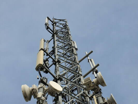 Telecommunication infrastructure has to provide high-bandwidth, high-quality and high availability systems for the massive numbers of everyday users. If you’re browsing for cat videos on your phone using 5G services, there is a high chance that an FPGA is used inside a base-station to encode and decode the data transmission between your phone and the cat video server. Since there are a multitude of communications standards which are evolving once every few years, FPGAs are a perfect match for radio base stations because they can be remotely reconfigured whenever needed.
FPGAs are used to perform a wide range of fast and complex mathematical transforms (Fourier Transform, Digital Filtering, etc…) and to create custom digital signal processing chains according to every applications needs. They can offer low-power, fast-to-market, reconfigurable capabilities for any radio / wireless protocol.
HIGH-FREQUENCY TRADING
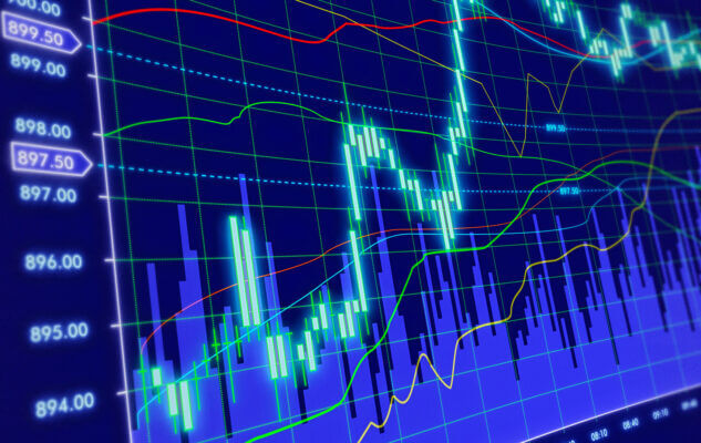 High-Frequency Trading (HFT) means to apply powerful math algorithms for stock exchange trading. The sole difference here is the astonishing speed these operations are performed which is in the nanoseconds range (1 second is 1 billion nanoseconds). In this fields the low-latency and high speed processing systems are key to large profits. While there are custom processors and servers designed specifically for this task, the low-latency and high processing power of an FPGA makes it ideal for this types of applications.
In this filed taking a decision a few tens of seconds later than your competition could mean high financial losses so taking it with a few tens of nanoseconds before you competition could result in massive profit. Another good example for FPGAs in the financial world is that JP Morgan implemented a High-Performance Computing cluster with FPGA accelerators that lets them analyze the risk of their trading transactions in near-real time.
ASIC PROTOTYPING
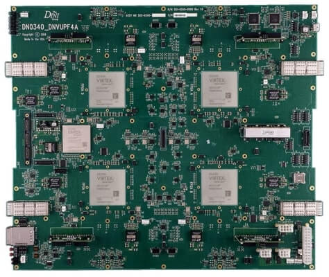 FPGA prototyping is the process of implementing/synthesizing an ASIC RTL code (Verilog or VHDL) on a physical platform that contains one or more FPGAs. These kind of platforms are used before tape out (sending the ASIC code to the factory) to check how your design responds to real-life stimulus. You can test a design with scenarios that are more complex that the ones you have simulated at RTL level. For example for, some protocols, simulating a 1ms of traffic using Modelsim (or other simulator) could take 2h, but on a real-life platform it will take 1ms. With these platforms you can find bugs that would occur only in heavy-duty real-life testing conditions.
Another role of these platforms is to start firmware development for the final chip way before the chip is mass produced. Since this is usually done by another department than the ones developing the chip, it bring a huge advantage in reducing overall costs and development time.
These development boards usually have multiple FPGAs, each having millions of logic cells (billions of transistors), with a total cost of hundreds of thousands of dollars. Even so their overall use brings costs reductions of millions if they are used efficiently.
CRYPTOCURRENCY MINING
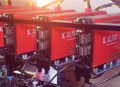 Because of the cryptocurrency revolution and blockchain hype people tried to find ways to mine these cryptocurrencies in a energy-efficient manner on devices that bring the maximum performance. Mining cryptocurrency means to find a solution to a complex mathematical problem and present it to a network before the other members. Initially this was done using your processor, but this was consuming lots of time and was not energy-efficient. The next step was to design ASICs that were extremely fast, but as the number o cryptocurrencies expanded, and the initial ones having algorithm updates, the equipment developers migrated towards GPUs and FPGAs. While GPUs are more power hungry and harder to find in stocks than an FPGA, this gives FPGAs a great profitability advantage over others kinds of chips.
This brought massive media exposure for FPGAs, gave them a piece of the hype the crypto stage is enjoying, and attracted development talent from other areas to FPGAs. FPGA mining is still a niche area in crypto mining because the mining workflow is considered to be extremely complex compared to ASIC / GPU mining.
WANT TO LEARN FPGA DESIGN?
As you can see there are many interesting high-tech fields where FPGAs are deployed and having a job there means and a wonderful career full of challenges and accomplishments, that also offers financial stability. The FPGA market is expected to grow with almost 10% per year until 2027 so there is a high need for professionals to fill these high-end jobs.
Working in FPGA design and verification is somehow similar to academic research and it involves a great imagination an creative problem-solving abilities. FPGAs are usually “programmed” using Hardware Description Languages and the one this blog is specialized is called Verilog HDL. FPGA design and Verilog as marketed as “difficult to learn”, or “complex”, but remember that it is NOT rocket science…
I had the same kind of problem when I started with FPGAs more 12 years ago and I had some hard times because I didn’t knew the technology, nor how a hardware description language works and how to code with it… I lost hundreds and hundreds of hours just to learn what I shouldn’t do… After a 10 years career in ASIC / FPGA design and verification plus a Ph.D in designing FPGA accelerators, I built this simple, hand-on tool that will help you master the secrets of Verilog very fast. If you are interested learning Verilog in a easy way, you can read more here….

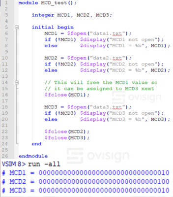 In this simple Verilog example, we can see how to declare three Multi-Channel Descriptors to open three files with them.
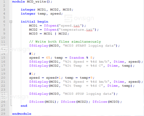 In this example, we are going to write the values of the temp and speed variables in speed.txt and temperature.txt. The test scenario is the following:
 First, create two files called data_in.bin and data_in.hex with the following content. Note that the files must be created at the same level where your simulator project is created (Modelsim in my case).
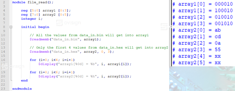
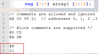 Let’s analyze a more complex data.txt format supported to load array1 using the command $readmemh(“data.txt”, array1):
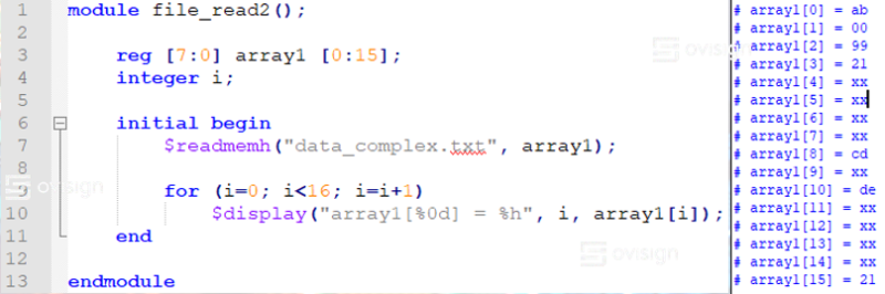

 This architecture consists of a rectangular array of logic blocks separated by channels containing routing resources (interconnects + switches). These blocks can be programmed to implement any desired function and are connected with the outside environment by using the I/O blocks. The function of the I/O blocks are used for tri-state control, output transition speed, pullp-up ori pull-down. The fastest interconnection is between adjacent blocks while the delay increases with the distance between the CLBs.
 The CLBs are grouped in rows with programmable interconnects placed between them. The I/O blocks are at the edge of the structure. Complex circuits are emulated by connecting adjacent rows via vertical interconnects.
 Hierarchical PLDs have a more complex layout. The top level is composed of logic blocks and interconnects. The logic blocks contain logic modules, which have combinatorial and sequential functional elements. The functional elements are controlled by the configuration bitstream stored inside the FPGA. The I/O blocks are placed at the edge of the system, shrouding the logic blocks and the interconnects.